NXP LPC1768 Software Developer
Who is a NXP LPC1768 Software Developer?
NXP LPC1768 Software Developer who design and develops software for NXP chipsets. He works mainly on freeRTOS or linux based software.
Are you looking for a nxp lpc1768 software developer for your projects. Then get in touch we can help with your project requirements.
About NXP
NXP Semiconductors Technology Microcontrollers arm LPC (MCUs) offer application performance and excellent developer experience. The LPC MCU family addresses all applications. All that ultra-low power solutions for primary control, ideal for eight, and replacing 16-bit advanced options for controlling digital signals supporting rigorous connectivity requirements. With over 400 arms with engines to choose MCUs, the NXP family offers one of LPC’s broader 32-bit ARM MCU portfolio, defined by exceptional ease of use, design flexibility, and advanced integration.
CHARACTERISTICS:
Comprehensive portfolio and an expansive ecosystem.
Most NXP LPC covered by the program produces MCUs NXP Longevity, ensuring the availability of a minimum of 10 to 15 years of product launch.
It should be supported by a coherent set of software and hardware development tools.
Low power without compromise, ideal for mobile applications.
It is available in a wide range of design flexibility packages, ultra-small chip packages, and tall quad flat packages.
Introduction about the topic
The LPC1768 has based micro controllers embedded applications with high integration and low power consumption level. The Cortex-M3 arm is a core that gives system improvements such as advanced debug features and an increased support block integration.
The LPC1768 operates at frequencies up to 100 MHz. The LPC1769 CPU operates at frequencies of up to 120 MHz. The Arm Cortex-M3 processor develops a three-stage pipeline and it then uses a Harvard architecture distinct local bus. The Arm Cortex-M3 processor also comprises an internal prefetch unit that supports speculative branching.
The peripheral complement LPC1768 comprises up to 512KB flash memory, a maximum of 64 KB of data storage, Ethernet MAC, USB Device / Host / OTG interface, general-purpose 8-channel DMA controller, four UART, two CAN channel, two SSP controllers, SPI, I2C bus interfaces 3, 2 + 2 inputs outputs of the I2S bus interface, an encoder interface quadrature four counters for general use, general-purpose 6-PWM output, energy ultra-low real-time Clock (RTC) with separate battery power and up to 70 general-purpose I / O pins S. The LPC1768 is pin-compatible with the Arm7 LPC236x-based 100-pin series of microcontrollers.
Features and Benefits
Arm Cortex-M3, operating at frequencies up to 100 MHz
(LPC1768) or a maximum of 120 MHz (LPC1769). Also, a Memory Protection
(MPU) supporting eight regions is included.
Up to 512 kB of the flash program memory chip. This also helps in acceleration improved flash memory of a high-speed operation of 120 MHz with nil wait states.
SRAM chip comprises:
32/16 kB SRAM on the CPU with local code/data bus for high-performance CPU
access.
2/1, 16 kB SRAM blocks with separate paths for higher throughput. These SRAM blocks can be used for Ethernet, USB, DMA memory, and general-purpose CPU instruction and data storage.
Eight general-purpose channel DMA controller (GPDMA) on the stack AHB
the matrix that can be used with SSP, I2S bus, UART, Analog-to-Digital, and Digital to analog converters devices, the timer matches signals, and transfers memory to memory.
Array interconnecting Multilayer AHB provides a separate bus for each AHB master. AHB masters include the CPU, DMA controller, general-purpose Ethernet MAC, and the USB interface. This interconnection allows communication without arbitration delays.
The split bus allows high throughput PDB with some stalls which are between the CPU and the DMA.
Serial interfaces:
Ethernet MAC with RMII interface and one suitable DMA controller.
USB 2.0 full-speed device / OTG controller with dedicated DMA controller and PHY chip to the host device, and OTG functions.
Four UART with fractional baud rate generation, internal FIFO, and DMA carrier. A UART modem control I / O and RS-485 / EIA-485 carrier and a UART IrDA have support.
2.0B CAN controller with two channels.
SPI controller with synchronous, serial, full-duplex communication.
There are two SSP controllers with FIFO and multi-protocol capabilities. PHC interfaces can be used with the GPDMA controller.
Three improved interfaces I2C bus, one with an open-drain output full support 2C specification and a fast mode plus data rates of 1 Mbit / s, both the standard port pin. Improvements include the recognition of multiple addresses and monitor mode.
2S interface (Inter-IC Sound) to the digital audio input or output, with fractional rate control. The I2S bus interface son supports three and data 4 son and receives, and the master clock enters to exit.
Other devices:
All GPIOs support a new configurable operation in an open-drain fashion. The GPIO section can be accessible by the multilayer AHB bus for easy access and present in the memory so that supports bands bit Cortex M3 and use by the general objective of the DMA controller.
The 12 bit analog to digital converter (ADC) with input multiplexing among eight pins, conversion rates up to 200 kHz, and multiple result registers.
The 10 bit digital to analog converter (DAC) with the help of a useful conversion timer and DMA support.
Four counters General Purpose/meters, with eight and ten capture inputs, compare results.
A motor control PWM AC motor control support.
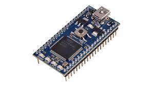
Interfaces available on LPC1768 Evaluation Board
The connectors of the LPC1768 evaluation board gives easy access to some of the LPC1768 chip peripherals.
USB 2.0 Full Speed interface: standard USB connectors for USB, USB OTG, USB, and UART host via USB on the LPC1758 board for applications that require USB communications.
Ethernet Interface: DM9000 series Ethernet controller chip is used for the Ethernet interface.
MicroSD Card Connector: MicroSD card connector for the development of applications requiring access to MicroSD cards.
TFT: A removable, 16×2 LCD can be used as a graphical display for displaying debug messages and the state of the real-time program.
Analog voltage for ADC Input command: An analog voltage source is adjustable on the LPC1768 plate to test the analog output function to the digital LPC1700. An active jumper configuration and disables this function.
JTAG and Cortex / ETM Download and Debug: The board LPC1768 integrates both a JTAG interface and a debug interface ETM Cortex +. Coupled with the USB-JTAG adapter ULINK2 the JTAG interface allows wireless serial flash programming and debugging. With the ULINKPro adapter, the debug interface Cortex / ETM allows flash programming and debugging instruction trace.
Read more about this.