AT32UC3A0512 ATMEGA32U4 Software Developer
Who is at32uc3a0512 atmega32u4 software developer?
at32uc3a0512 atmega32u4 software developer is a engineer who works on atmel based AVR chipset. He is involved in designing and developing custom application using C or C++.
Do you need at32uc3a0512 atmega32u4 software developer for your projects. Then get in touch we can help with your projects.
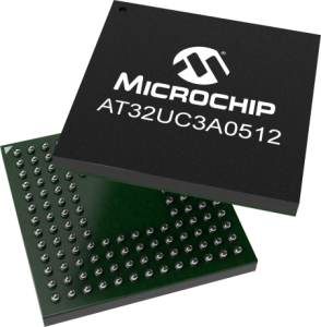
Introduction about AT32UC3A0512
The AT32UC3A is a micro controller known as a reliable chip based on the AVR32 with RISC architecture processor that can be clocked at frequencies up to 66 MHz. AVR32 UC is a good performance 32-bit RISC micro controller core designed for embedded applications, while consuming low power, high code, and high performance density. The processor will now implement a Memory Protection Unit (MPU) and a fast and flexible interrupt controller, which will help in supporting modern operating systems and operating systems in real-time. Higher computing capabilities are achievable using a set of DSP instructions.
Working of AT32UC3A0512
The AT32UC3A integrates on-chip Flash and SRAM for secure and easy access. The device’s direct memory access controller (PDCA) allows data transfer between peripherals and memories without processor intervention. PDCA significantly reduces treatment head when transferring continuous data flows and large between modules within the MCU. PowerManager improves design flexibility and security: the chip Brown-Out Detector monitors the power supply, trails of the CPU of the RC oscillator on-chip or external of oscillator sources, a real-time clock and its associated clock keeps track of the time.
The timer/counter comprises a three-channel timer/counter with 16 identical bits. Each channel can be independently programmed to measure the frequency, the counting of events, the measurement interval, the pulse generator, the delay time, and pulse width modulation. The PWM module offers various independent channels with many configuration options, including polarity, alignment edges, and the waveform non-overlap control. A PWM channel can trigger ADC conversions for loop control implementations closed more accurately. The AT32UC3A also has numerous communication interfaces for intensive communication applications. In addition to standard serial interfaces such as UART, SPI, or TWI, like other interfaces, synchronous flexible Serial controller, USB, and Ethernet MAC are available.
The synchronous serial controller allows easy access to serial communication protocols and audio standards, such as I2S. The Full-Speed USB 2.0 supports multiple USB device interface classes together, thanks to the rich endpoint configuration. On-The-Go (OTG) host interface allows the device like a USB flash drive or USB printer connected directly to the processor. The carrier-independent interface (MII) and Reduced MII (RMII) 10/100 MAC Ethernet module provides on-chip solutions for devices connected to the network. AT32UC3A incorporates on chip debugging, with a track in real-time, full read / write memory access, and more control access to the basic design.
Features of AT32UC3A0512
High performance, low power 32-bit AVR® Microcontroller
Compact single-cycle RISC instruction set of instructions, including DSP.
Modify read-write instructions and atomic bit manipulation.
Execution 1.49 DMIPS / MHz.
Up to 91 DMIPS current at 66 MHz from Flash (one wait state)
Up to 49 DMIPS at 33MHz draft from Flash (0 wait state)
Memory Protection Unit
Multi-hierarchy system bus
The high-performance data transfers on separate buses for better performance and results.
15 DMA channels improve peripheral speed to peripheral communication.
Internal High-Speed Flash
512K bytes to 256K bytes to 128K bytes Versions.
Single-cycle access up to 33 MHz.
Prefetch buffer Optimizing Executing at maximum speed.
Programming time 4ms and 8ms page full-time Chip Clear.
One hundred thousand write cycles, 15 years of data retention efficiency.
Flash Security Locks and Configuration area defined by the user.
External Memory Interface product derivatives AT32UC3A0
SDRAM / SRAM compatible memory bus (24-bit data and 16-bit address bus)
System functions
Power and Clock Clock internal RC Manager and including a 32KHz Oscillator.
Two Oscillators multipurpose and two Phase-Lock-Loop (PLL) for independent USB CPU Frequency Frequency.
Watchdog, real-time clock timer.
Introduction about ATMEGA32U4
ATMEGA Microcontroller belongs to the AVR microcontroller family, and Atmel Corporation makes it. Also. ATMega Microcontroller is an 8-bit microcontroller with a reduced instruction set (RISC) based on Harvard architecture.
It has standard features such as the ROM chip (Read Only Memory), data RAM (Random Access Memory), data of EEPROM (only programmable electrically erasable memory dead), timers and Ports input/output, as well as additional devices as an analog to digital converters (ADC) interface Access series, etc. They set 120 and several beaches and the program memory of the instruction 4K to 256K bytes.
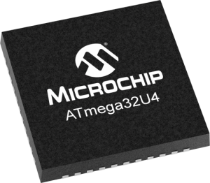
Two students designed the microcontroller ATMEGA at the Norwegian Institute of Technology (NTH) – Alf Bogen and Vegard-Nigel Wollan. It was then purchased and developed by Atmel Corporation in 1996.
ATMEGA Microcontroller Architecture
As mentioned in the introduction, the ATMEGA microcontroller is based on Harvard architecture, namely the separate data memory and program memory. The memory, also known as program code or program memory name, is random access flash memory (ROM). The size of the program memory is between 8 K to 128 K bytes.
The data memory is divided into three parts – 32 general registers, input/output memory, and internal static random-access memory (SRAM). While the general-purpose registers’ size is fixed, the I / O memory and the internal SRAM size vary from chip to chip.
Features of ATMEGA32U4
High performance, low power AVR® 8-Bit Microcontroller
Advanced RISC includes:
135 – useful instructions, more straightforward clock cycle execution.
32 x 8 General Registers to work on.
Operations are fully-static.
Up to 16 MIPS Throughput at 16MHz.
On-Chip 2 Multiplier cycle.
Non-volatile Program and data memories include:
16/32 Kbytes of In-System Programmable Flash self.
1.25 / SRAM internal 2.5 kb.
512bytes / internal EEPROM 1KB.
USB Device 2.0 full-speed / low-speed module with interruption of the transfer completion:
It assembles with the Universal Serial Bus Specification Rev. 2.0
It supports data transfer rates up to 12 Mbit / s and 1.5 Mbit / s
Setting 0 for control transfers: up to 64 bytes.
Six Programmable Endpoints with or rear directions and with bulk or interrupt.
Size Endpoints Configurable up to 256 bytes in double bank fashion.
Fully independent 832 bytes DPRAM for USB endpoint memory allocation.
Suspend / Resume Interrupts.
Acknowledge CPU detection possible on the USB Bus Reset.
PLL 48MHz bus for full-speed operation.
USB connection Bus / Disconnection on request Microcontroller.
Operation Crystal-less for the low-speed mode.
Device Features
PLL USB chip and high-speed timer 32 operations up to 96 MHz.
An 8-bit Timer / Counter with separate Prescaler and Compare Mode.
Read more about this.